Introduction
Welcome to our comprehensive guide on the ZCU102, a powerful and versatile development board that offers exceptional capabilities for a wide range of applications. In this article, we will delve into the intricate details of the ZCU102 and provide you with valuable insights and knowledge to help you make the most of this remarkable platform. Whether you’re a seasoned developer or a newcomer in the field, we’ve got you covered. So, let’s embark on this enlightening journey together!
Unleashing the Power of the ZCU102
An Overview of the ZCU102
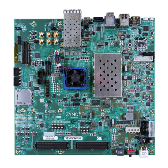
The ZCU102 is an advanced development board manufactured by Xilinx, designed to unleash the full potential of their cutting-edge Zynq UltraScale+ MPSoC (Multi-Processor System on Chip) technology. It combines the power of a high-performance application processor with the flexibility and programmability of an FPGA (Field-Programmable Gate Array). This unique combination empowers developers to create highly optimized and customized solutions for a myriad of applications.
Unparalleled Processing Power
At the heart of the ZCU102 lies the Zynq UltraScale+ MPSoC, which integrates a quad-core ARM Cortex-A53 processor along with a dual-core ARM Cortex-R5 real-time processor. These processors provide a substantial amount of computational power, enabling the board to handle complex tasks with ease. Whether you’re working on artificial intelligence, embedded vision, or high-performance computing projects, the ZCU102 is more than capable of meeting your demanding requirements.
Versatility for Various Applications
The ZCU102 offers exceptional versatility, making it suitable for a wide array of applications. From edge computing and IoT (Internet of Things) devices to advanced robotics and aerospace systems, this development board can be tailored to meet the unique needs of any project. Its FPGA fabric allows for hardware acceleration, enabling developers to optimize performance and achieve real-time responsiveness, making it an ideal choice for applications that require low-latency and high-bandwidth data processing.
Uncompromising Connectivity
Connectivity is crucial in today’s interconnected world, and the ZCU102 doesn’t disappoint in this aspect. It provides a rich set of interfaces and connectivity options, including USB 3.0, Gigabit Ethernet, HDMI, DisplayPort, PCIe, and more. These interfaces allow seamless integration with various peripherals, sensors, and external devices, facilitating the development of comprehensive and interconnected systems.
Getting Started with the ZCU102
Setting Up the Development Environment
To kickstart your journey with the ZCU102, it is essential to set up your development environment properly. Here’s a step-by-step guide to get you up and running quickly:
- Acquire the ZCU102: Purchase the ZCU102 development board from an authorized distributor or directly from Xilinx.
- Install Vivado Design Suite: Download and install the latest version of Xilinx Vivado Design Suite, which provides a comprehensive set of tools for designing, implementing, and debugging FPGA-based systems.
- Board Setup: Connect the necessary peripherals to the ZCU102, such as a power supply, monitor, keyboard, and mouse.
- Connectivity: Establish a connection between your development machine and the ZCU102 using an Ethernet cable or a USB cable, depending on your preferred communication method.
- Initialize the Board: Power on the ZCU102 and ensure that it boots up correctly. Familiarize yourself with the board’s LEDs and switches, as they can provide valuable feedback during the development process.
Exploring the ZCU102 Features
Now that you have your development environment set up, let’s dive into the various features and components that make the ZCU102 an exceptional platform for your projects:
Processing System (PS)
The Processing System (PS) in the ZCU102 comprises the ARM Cortex-A53 and Cortex-R5 processors, providing a combination of application processing and real-time processing capabilities. The PS handles tasks such as running the operating system, executing software applications, and managing external interfaces.
Programmable Logic (PL)
The Programmable Logic (PL) section of the ZCU102 houses the FPGA fabric, which allows developers to implement custom hardware accelerators and peripherals. The PL can be programmed using Xilinx Vivado, providing immense flexibility and customization options to meet specific project requirements.
Memory Interfaces
The ZCU102 offers various memory interfaces, including DDR4 memory banks, Quad-SPI flash memory, and SD card slots. These interfaces enable efficient storage and retrieval of data during runtime, ensuring smooth and reliable operation of your applications.
High-Speed Interfaces
With high-speed interfaces such as USB 3.0, Gigabit Ethernet, DisplayPort, and HDMI, the ZCU102 ensures seamless connectivity with external devices and systems. These interfaces enable rapid data transfer, real-time video processing, and the integration of multiple peripherals into your projects.
JTAG Debugging
The Joint Test Action Group (JTAG) interface available on the ZCU102 facilitates debugging and testing of your designs. Using JTAG, developers can interact with the ZCU102 at a low-level, allowing for efficient troubleshooting and verification of their FPGA designs.
Conclusion
In this comprehensive guide, we have explored the remarkable capabilities of the ZCU102 development board. From its powerful processing system to its versatile programmable logic, this platform provides developers with immense potential for creating innovative and optimized solutions. With its uncompromising connectivity options and a wide range of high-speed interfaces, the ZCU102 empowers developers to build interconnected systems that push the boundaries of what is possible. Now equipped with this knowledge, you are ready to embark on your own ZCU102 journey and unleash your creativity in the world of advanced embedded systems.